


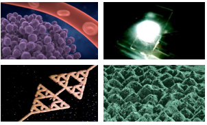
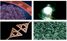
THE OPTIMIZATION OF MOLECULAR STRUCTURES TO CREATE INDUSTRY-
TRANSFORMING PRODUCTS - EFFECTIVELY IMPROVING QUALITY OF LIFE
AND REDUCING THE FOOTPRINT OF PRODUCT SUPPLY CHAINS.

OUR MISSION


Why Applicote?


STRATEGIC PARTNERS


PATENT PORTFOLIO ALLOCATION

Contact


SOCIAL MEDIA

PARTNER SITE LOGIN


CONTACT
Main: 407.474.4269
Fax: 800.390.3032
e-mail: info@applicote.com
PHYSICAL ADDRESS
4304 Scorpius St, Bldg 53
Orlando, FL 32816-2700
MAILING ADDRESS
P.O. Box 162700
Orlando, FL 32816-2700

© Applicote Associates, LLC, All Rights Reserved.


Executive Leadership

SENIOR EXECUTIVES

ADVISORY BOARD MEMBERS
|
Note:
To
use
the
above
contact
features,
please
select
a
default
e-mail
program
if
you
have
not
already
done
so.
If
prompted,
allow
the
website to notify your e-mail program to initiate a new message.


THE OPTIMIZATION OF MOLECULAR
STRUCTURES TO CREATE INDUSTRY-
TRANSFORMING PRODUCTS -
EFFECTIVELY IMPROVING QUALITY OF
LIFE AND REDUCING THE FOOTPRINT
OF PRODUCT SUPPLY CHAINS.

OUR MISSION


Whether you need a CRO with unique capabilities, unrivaled HPLI derivative R&D, or access to IP that will immediately transform your marketplace, Applicote is a unique and forward-thinking solution.
Learn more about how we can quickly help resolve design and process limitations and move your products to the leading edge of the marketplace.


SENIOR EXECUTIVES

ADVISORY BOARD MEMBERS

What We Do
Why Applicote?
Executive Leadership

Industrial Applications

STRATEGIC PARTNERS


PATENT PORTFOLIO ALLOCATION


Contact
SOCIAL MEDIA
PARTNER SITE LOGIN


PHYSICAL ADDRESS
4304 Scorpius St, Bldg 53
Orlando, FL 32816-2700
MAILING ADDRESS
P.O. Box 162700
Orlando, FL 32816-2700

© Applicote Associates, LLC, All Rights Reserved.
|